The problem form Computer Engineering Department from Iraq using VHDL

A solution of problem #1:
First, we have to design the flip-flop JK as is shown in figures 1 and 2.
After that, we have to design and connect the components with the flip-flop.
JK Flip Flop
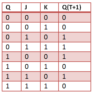
Figure 1. True table.
library IEEE;
use IEEE.STD_LOGIC_1164.ALL;
entity JK_Flop is
Port ( J : in STD_LOGIC;
K : in STD_LOGIC;
clk : in STD_LOGIC;
Q : out STD_LOGIC;
QN : out STD_LOGIC);
end JK_Flop;
architecture Behavioral of JK_Flop is
signal data: std_logic :='0';
Begin
process (clk, J, K) begin
if (clk'event and clk = '1') then
if(J='0' and K='0')then
data <= data;
elsif (J='1' and K='1')then
data<= not data;
elsif (J='0' and K='1')then
data<= '0';
else
data<='1';
end if;
end if;
end process;
Q <= data;
QN <= not data;
end Behavioral;

Figure 2. Flip-flop JK simulation.
Second:
The solution of problem #1 by top-level design.
------------------------------------------------------------------------------------------------------------------
library IEEE;
use IEEE.STD_LOGIC_1164.ALL;
entity top_desing_1 is
port (
RA: in std_logic;
RB: in std_logic;
clk: in std_logic;
EA, EB: out std_logic
);
end top_desing_1;
architecture Behavioral of top_desing_1 is
COMPONENT JK_Flop
PORT(
J : IN std_logic;
K : IN std_logic;
clk : IN std_logic;
Q : OUT std_logic;
QN : OUT std_logic
);
END COMPONENT;
signal not_RA: std_logic;
signal not_RA_and_RB: std_logic;
signal not_RB: std_logic;
signal noty1: std_logic;
signal RA_or_RB: std_logic;
signal not_RA_and_not_RB: std_logic;
signal y2: std_logic;
signal not_y2: std_logic;
begin
not_RA_and_RB <= not_RA and RB;
not_RB <= not RB;
Inst_JK_Flop: JK_Flop PORT MAP(
not_RA_and_RB,--J
not_RB,--K
clk,
EB,--Q
noty1--QN
);
not_RA <= not RA;
not_RB <= not RB;
RA_or_RB <= RA or RB;
not_RA_and_not_RB <= not_RA and not_RB;
Inst_JK_Flop2: JK_Flop PORT MAP(
RA_or_RB,--J
not_RA_and_not_RB,--K
clk,
y2,--Q
not_y2--QN
);
EA <= noty1 and y2;
end Behavioral;
------------------------------------------------------------------------------------------------------------------
The solution by the RTL schematic is shown in figure 3.

Figure 3. RTL top design of problem1.


No hay comentarios.:
Publicar un comentario